
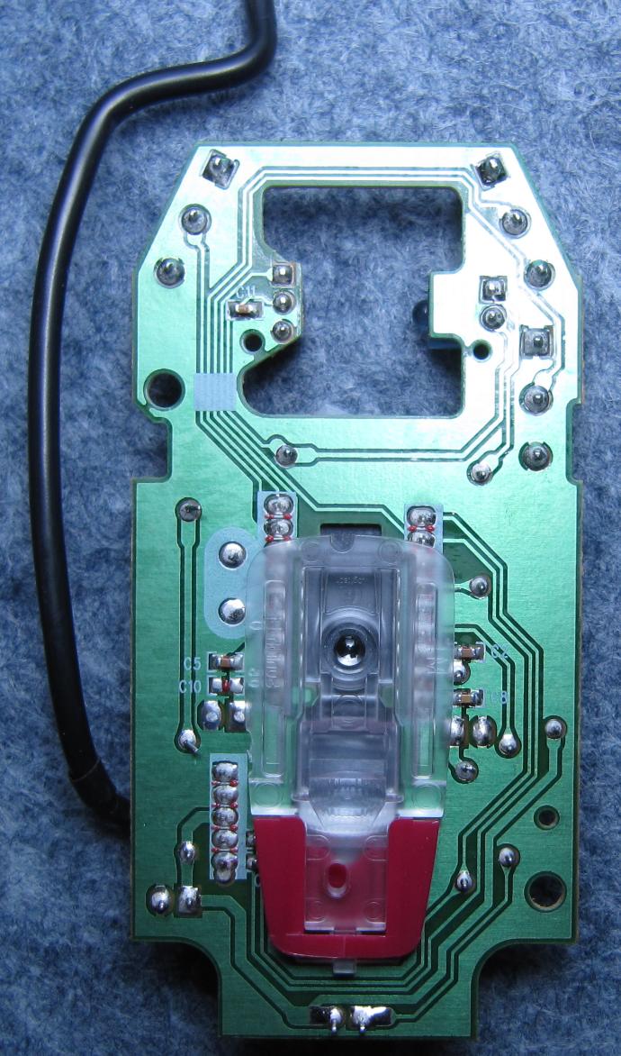
This entry will have more to say about the printed circuit boards that replaced the point-to-point wiring discussed in the last entry. I'll talk a bit about how they are assembled and soldered, and how their density has increased over the years. I included photos of the mouse board to show the "printed" wiring, with the leads sticking through the board from the other side (the component side) soldered to the copper traces. The small mounds of solder at each connection point show up as silvery dots on the image. If you click on it to enlarge it, and then click again to make it even bigger, you can see the wire leads coming through from the other side, sticking out from some of the dots (return here with your "Back" button). Replacing actual wires with a printed circuit saves a lot of labor in itself, but soldering each connection by hand would still involve a lot of labor. The mouse board is very small - it's only 8 cm long by 4 cm wide (3 1/8 X 1 9/16 inches). It has to be small, because it has to be mounted inside a mouse which fits under your hand. But most boards are larger, with connections numbering in the thousands. So a process was developed for making the solder connections almost all at once. It's called "wave soldering".
The printed-circuit board shown, with its component leads inserted into the holes in the board, is being carried along by the metal fingers you see in the photo. It first travels over a pre-heater, and then is carried over the wave. The solder wets the component leads and exposed copper traces, and is wicked up into any holes in the board. All connections on the board are completed in seconds. Although I glossed over this in my previous entry, the green "mask" on the bottom of the mouse board is actually a "solder mask", designed to keep solder from adhering to the board anywhere but at the connection points, where the component leads protrude through the board. All the processes of making a completed printed-circuit board are heavily automated. After creating the board, holes of various sizes are drilled by a computer-controlled drill, and the components are inserted by an automatic insertion machine. Finally, the boards are fed through the wave-soldering machine, and then generally washed in deionized water. There's an effort these days to make electronic products compact. Certainly, that's a necessity with things like cellular telephones (I'll talk a bit more about them later in this entry). But let's step back in time a bit, to 1964. Early on, there wasn't much pressure to pack components densely. Look just below at a portion of a printed circuit board from that year: 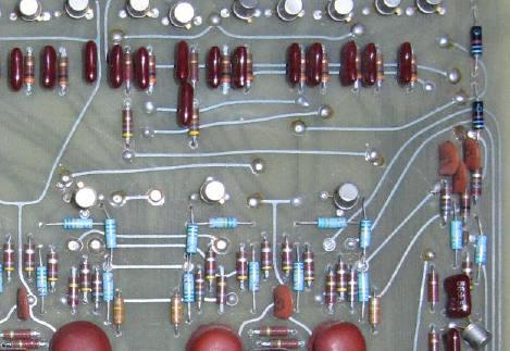 The board shown is from a PDP-6 mainframe computer. You can click on the picture to see the entire board, which is quite large, about 27 X 24 cm (10.6 X 9.4 inches). The section of the board shown above is about 12 X 8 cm (4.7 X 3.2 inches). On my monitor, the picture above is about 15 percent larger than actual size. My objective in giving these dimensions is simply to point out that the printed wiring on this board is not at all dense. It's clear that in this expensive mainframe computer, which contained hundreds of these boards, no effort was made to make the product compact. I should also point out that the silvery circles seen in the picture are the tops of individual "discrete" transistors. That is, each of these small metal cans contains a single transistor. Of course, if all the "wiring" is on one side of a flat board, it's not possible for one wire to cross over another. But unlike the mouse board, this board has conductive traces on both sides - in the picture, you can see the faint outline of traces on the opposite side of the board. Electronic circuits with any complexity must be built with at least two layers of circuitry. The best layout of the conductors is obtained when most of the conductors on one side of the board go lengthwise on the board, while the conductors on the opposite side go crosswise. To make connections between the opposite sides of a two-sided board, a method was developed to metal-plate the inside of the holes drilled through the board, allowing these holes to conduct electricity from one side to the other. Then, as the technology developed further, additional layers were added in the middle - printed circuit boards these days typically have up to seven conductive layers, each potentially contacting selected plated-through holes. But as you can see from the mouse board at the top of this entry (it's only a few years old), single-sided boards are still used where possible - they're much less expensive. As the state-of-the-art of electronic packaging and interconnection continued to develop, the number of components that could be packed into a given volume of space continued to increase. Printed circuit boards got more dense, with many more thin traces packed into the available real estate. Indeed, nowadays, the "through-hole" technology I've described above is less frequently used for really compact products. Rather a technique called "surface mount" is used, in which components in very small packages are connected to small solder-bumps on the component side of the board only. But through-hole boards were still the dominant technology when I built my Heathkit/Zenith Z-150 computer, a PC clone, in 1984. The board below shows a typical density at that time - the picture shows the Memory board from that computer. 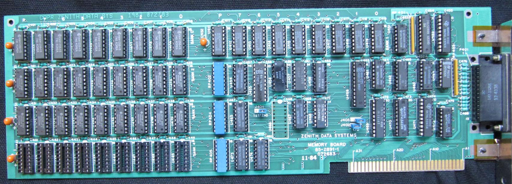 The board shown above is 36.2 cm wide by 11.25 cm high (14.25 X 4.44 inches). The black rectangular devices are digital "integrated circuits", sealed into a type of package called a "DIP" ("Dual In-line Package" - click the link for a Wikipedia article). They are plugged into sockets which are soldered onto the board. You can see a row of empty sockets at the bottom left - they represent a part of the memory array that was not "populated" with DIPs, but the sockets were soldered in place to allow for future expansion. The next picture shows the back side of the same board: 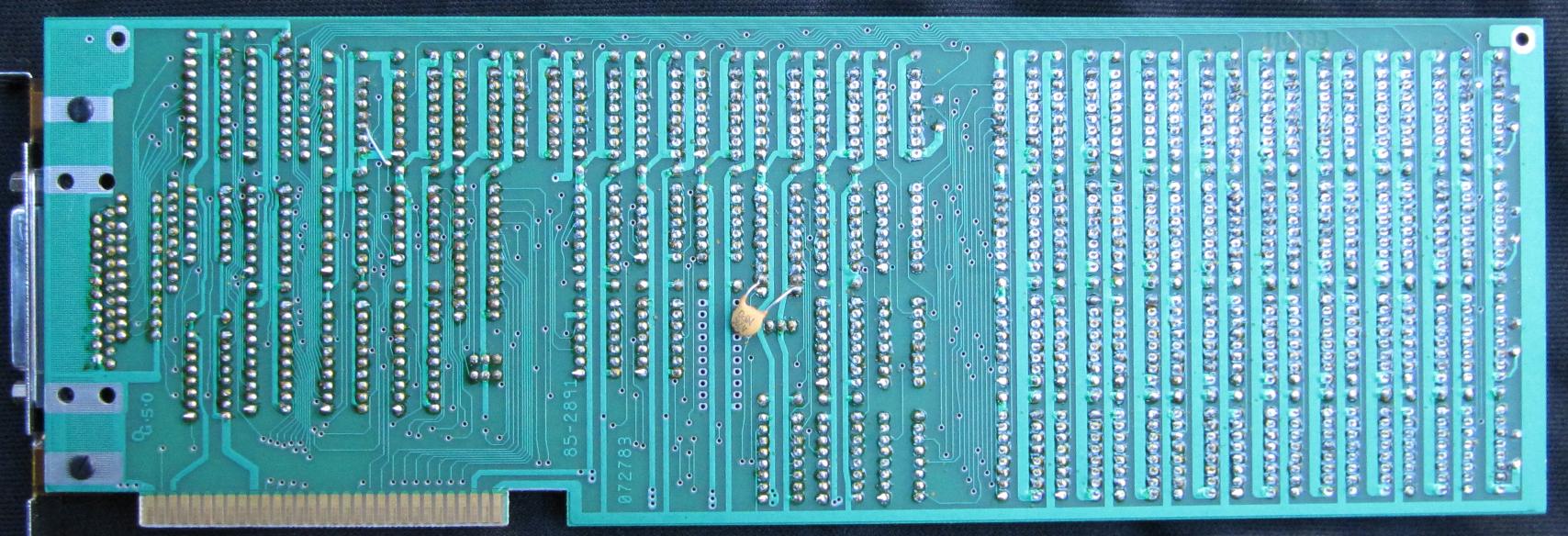 Although wave soldering was certainly available at the time I build this board, it's not something one can do at home - it takes a very large and expensive machine, and a trained operator. Since I built the computer from a kit, I was the one who inserted all the components, and the soldering has to be done after the component insertion. Thus I had to hand-solder every single one of those silvery dots, each of which connects a single pin of an integrated circuit socket, or some other component, to the board's wiring. Note 2
The even smaller silvery circles with black dots in the center (you'll need to click either the front or back board pictures above to enlarge it to see those) are smaller plated-through holes that don't have a component lead in them, but which are just making front-to-back connections. Because proper soldering was crucial to successful building of the computer, the construction steps began with a soldering course. This allowed the builder to get actual practice soldering before starting work on the actual PC boards. Click here to see the first three pages of that course, copied from the manual, which include the PC board cross-section diagram just above. A large increase in component packing density in electronic products was due to the development and refinement of the printed-circuit board. But a much larger increase was due to the development of the integrated circuit. To make integrated circuits, techniques were developed for putting multiple transistors and other components on a single "chip", forming them on a semiconductor base, generally made of highly purified silicon. For technical reasons, this technology prove to be particularly suited to digital circuitry. In short order, digital circuits containing tens of thousands of transistors were being built, then circuits with hundreds of thousands, then millions, and then more. Note 3 The wires in the radio I described at the beginning of this entry, purchased by my grandfather Abe in 1955, connect nine vacuum tubes, and probably a hundred or so other components. It contains essentially two radio receivers, one to receive AM (Amplitude Modulation) signals, and one to receive FM (Frequency Modulation) signals in a different frequency range. My Zenith PC contains, I'd estimate, about 150 integrated circuits, but internally, each of them probably comprises several thousand transistors. These would now be described as SSI (Small Scale Integration) and MSI (Medium Scale Integration) circuits. But consider my Samsung Galaxy S III "smart phone". It contains a powerful computer, integrated onto a single chip which probably contains in excess of a billion transistors. It contains over 30.8 gigabytes of memory (that's over 33,071,248,179 bytes). The Z-150 memory board shown above, after I expanded it with higher-capacity chips that became available somewhat after it was built, held 320 kilobytes (327,680 bytes). The Galaxy S III has a high-resolution touch-sensitive color display, and two built-in cameras, one of which contains an image detector with about 25,000 separate light-sensors (pixels). The phone also has a GPS radio receiver (Global Positioning System) capable of picking up minute signals from multiple satellites orbiting hundreds of miles overhead. It has a telephone transceiver (transmitter/receiver) that can operate on multiple bands. It has a short-range Wi-Fi transceiver, and an even shorter range Bluetooth transceiver. So in all, it has four separate radio receivers, and three separate transmitters. Each needs an antenna, and they must not interfere with each other. Within and surrounding the integrated circuits, it contains billions of separate connections of various sorts, and all of it fits in my hand. It's interesting how much people take this technology for granted these days. There's an incredible amount of work behind it. Moore's Law doesn't hold up by magic. Doubling the number of transistors on a chip every two years means that in that time, engineers have to improve their fabrication techniques by a factor of two, and then again two years later, and then again, and then again, and then again. If you're a semiconductor company, and you don't manage it? You're bankrupt, left behind. Yet people give this almost no thought. Two-year-olds take it for granted. But I can't take it for granted. I've seen it happen.   Note 1: In case you're curious: the red and translucent component you see towards the bottom is an optical assembly holding an illuminating LED (Light Emitting Diode) and a lens used to focus an image of the mouse pad onto a sensor in the integrated circuit on the component side. The black wire heading up to the top of the picture goes off to a USB connector. The cutout in the top of the board was to provide space for the bottom of the scrolling wheel between the two mouse buttons. This particular mouse was made by Dell. After many years of service, it began to malfunction by occasionally producing a double-click when I had pushed the left button only once. This produced problems in quite a few software applications. I replaced it with a wireless mouse, and of course, being me, I took the old one apart. [return to text] Note 2: That small yellow thing in the center of the back of the board is an electronic component called a "capacitor". No doubt Heathkit/Zenith found out it was needed after the boards had been fabricated, so they included instructions in the kit to add it to the circuit. And the easiest place to add it must have been on the back of the board, so there you have it. If you've got a sharp eye, you might have also noticed a short wire added to the back of the board, at the upper-left. Again, some sort of correction made after the board had been fabricated. Do you have a really sharp eye? Look back at the underside of the mouse PC board, the first image shown above. There are several capacitors of a different type mounted on the underside of the board, tiny "chip" capacitors, made to be surface mounted. The ones you can see are labeled C2, C5, C8, C10, and C11. They're on the bottom of this board because it's only one-sided, and they're components designed for surface mounting. They probably had to be soldered on by hand after the board had been wave-soldered. This is called a "secondary operation". [return to text] Note 3: The techniques used to make integrated circuits are not unlike those used in making printed circuit boards. It's photo-lithography - successive masking steps to create multiple layers in the silicon (often hundreds of steps). But the scale is entirely different - the elements of these circuits are microscopic. The tiniest speck of dust will destroy a circuit, so operations are done in dust-free "clean rooms". Multiple circuits are created all at once on large "wafers" of highly-purified silicon. If you want to learn more, here's a decent History of the Integrated Circuit, including an overview of the production steps. You might also take a look at the Wikipedia article. The steady increase in the number of transistors that could be put onto a single chip became known as "Moore's Law", first articulated by Gordon Moore, one of the co-founders of the semiconductor company Intel. He observed that historically, the number of transistors that manufacturers were able to fabricate on a single chip had roughly doubled every two years. This "rule" has approximately continued - see Wikipedia again for a good article on Moore's Law. Take a look at the graph on the right in that article. [return to text]  |
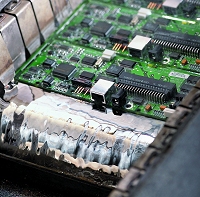 The image to the right gives you an idea of how the process works. Molten solder is pumped up through a slot, producing a silvery "wave" of solder with a rounded top. You can see the wave towards the bottom of the picture.
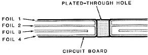 The printed-circuit boards (PC boards) used in my computer had up to four layers of conductive copper foil (I called these "traces" above), all connected as needed by holes drilled through the board which were then metal-plated (see a diagram of a board cross-section to the left).