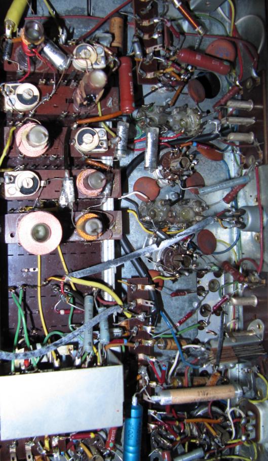
 Initially shown in the United States in 1979, James Burke's documentary television series Connections “... took an interdisciplinary approach to the history of science and invention and demonstrated how various discoveries, scientific achievements, and historical world events were built from one another successively in an interconnected way to bring about particular aspects of modern technology.” Note 1 My goals here are much more modest. In a couple of blog entries, I'm going to spend a bit of time discussing how the methods of making connections in electronic circuitry have changed during my lifetime. While I'm hardly going to do an exhaustive review, I hope I can give you an idea of what has happened over the decades I've witnessed. As you may know, some materials (generally metals) conduct electricity, while other materials do not (they are called insulators). Building electronic circuits involves creating paths to carry electrical current from one component to another. This has been done in various ways over time. 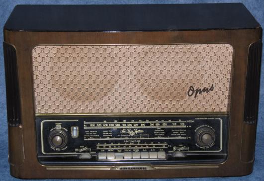
Tipping it up and removing a small cover on the bottom reveals how the components are wired together. They're connected by actual wires, which are joined where necessary by stripping off their insulation, and connecting them by a process called "soldering". This is done by fusing a low melting point alloy of lead and tin called "solder" at the point where the conductors meet. By the way, in the word "solder", the L is sounded in British English, but is silent in American English (we Americans pronounce it as if it were written "sodder"). The soldering of circuits built like this radio was done by hand. After all, electricity was always carried by wires. What more obvious way to link electronic components than to connect them together with wires? Soldering wires together produces a reliable electrically conductive joint.
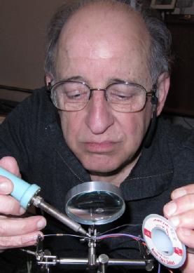
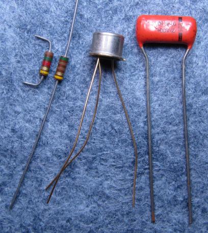
To the right, a quick demo for you. I'm holding the hot soldering iron in my right hand (to your left), and a spool of solder (in the form of a wire) in my left hand. There are many fixtures available to hold wires and electronic components in place while they're being soldered. I'm using a simple one that uses "alligator clips" to hold the wires. It also provides a magnifying glass to help me see what I'm doing close up. The wires being joined can't simply be embedded in a glob of solder. They need to be themselves heated, so that they will be "wet" by the molten solder before it cools. A poorly made solder connection is called a "cold solder joint", generally occurring because the wires being connected were not adequately heated. On the other hand, if you overheat the "lead" of an electronic component (the wire that connects it to the circuit), you can damage the component. You need to heat a connection enough fuse the solder to the wire, but no more. A good soldering iron is thermostatically controlled, so it always maintains the proper temperature. Some electronic components can be seen to the left. Left-to-right, they are two resistors, a transistor, and a capacitor. The "leads" are the wires protruding from the body of the component. In that context, the word "lead" is pronounced LEED, while the name of the metal "lead" is pronounced LED. Ah, such is English. The left-most resistor in the picture has had its leads clipped short, and bent over, probably for insertion into a printed-circuit board, to be discussed below. Here's a close-up of the connection I made, before and during soldering:  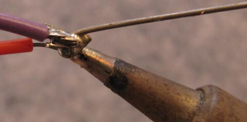 But for electronics to have a future, a means had to be found for connecting more and more components, in smaller and smaller volumes, using less and less labor. Numerous ways were developed for doing this, but by far the most important method was the "printed circuit". Look at the small printed circuit board just below. It's actually a board from a defunct optical computer mouse. The top side of the board, called the "component side", is on the left. The bottom side, with the printed circuit, is on the right:  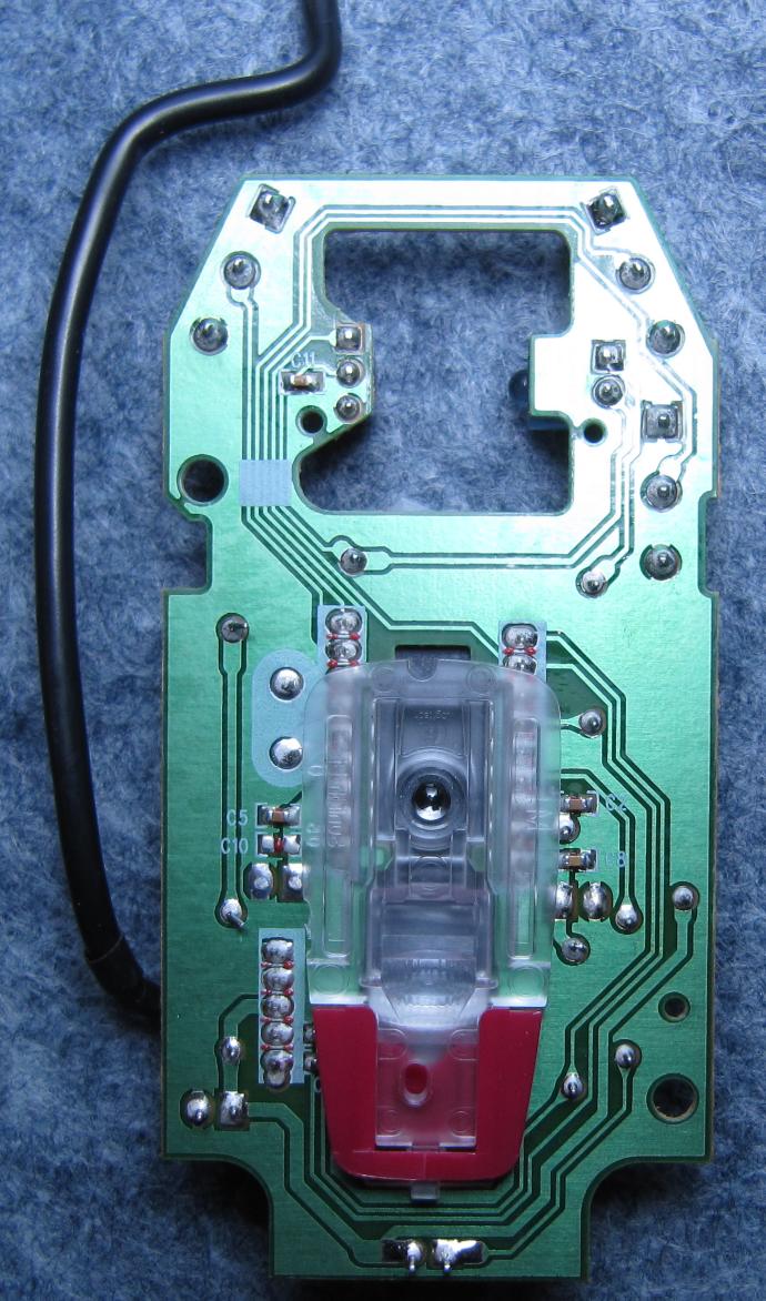 The components seen on the left include resistors, capacitors, and Light-Emitting Diodes (LED's). The three black rectangles at the top are switches, one for the left mouse button, one for the right, and one to sense depression of the scrolling wheel between the two buttons. The larger black rectangle in the middle, with eighteen legs arranges in two rows (a so-called Dual Inline Package, or "DIP), contains the integrated circuit that does most of the work. The component leads go through holes in the board to the bottom, where they are soldered to the printed wiring, as seen on the right. In fact, those solder connections are what hold the components down on the board, in addition to making electrical connections. The thin silvery lines that you can see on the bottom side are the "wires". They are not literally wires, but rather are "traces" of conductive copper. The copper has been plated with a silvery-looking coating to keep it from oxidizing, and then all the traces have been covered with a semitransparent green insulating and protective mask, except in the areas where the component leads have been soldered. Note 2 In my next blog entry, I'll discuss how the solder connections on the bottom of the board are all made almost at once, by a process called "wave soldering". My sister Phyllis once got a summer job in some lab at MIT, so she stayed with me in my apartment in Cambridge that summer. At some point, the lab needed to have some electronic boards hand-assembled, which involved soldering components onto a set of identical printed-circuit boards. In a group meeting, the employees were asked if anyone knew how to solder. Phyllis raised her hand - she had learned to solder in order to make silver jewelry (soldering silver takes a special type of solder made specifically for that purpose). So Phyllis was given a bunch of empty ("unpopulated") printed-circuit boards, boxes of components, and a finished sample board to work from. She then "cloned" the sample board, picking out identical components for each position, bending the leads to the appropriate lengths, inserting them through the holes in the board, and soldering them on the bottom side. Observing some of her completed boards, I noted that she really didn't have to have all the resistors facing the same way, with the colored stripes on the same side as the sample board. Resistors are bi-directional, so they can face either way. But then she asked about the diodes, which looked a bit like the resistors, but with different markings. Uh-oh, the direction of mounting does matter for the diodes. Phyllis decided to just copy everything exactly, so that her boards looked precisely like the sample board in every respect. They were beautifully done. And they worked. Next blog entry: More about printed circuit boards, leading up to the boards I assembled for my first personal computer. It's been previously mentioned in an entry called Personal computers - I built it from a Heathkit.   Note 1: From the Wikipedia entry on Connections. [return to text] Note 2: These boards are not literally printed, despite the name. Creating them typically involves laminating a thin layer of copper to a board (generally made out of a fiberglass epoxy, for rigidity and long life). The copper is then coated with a layer of a photosensitive "resist", which hardens (polymerizes) when exposed to ultraviolet light. The board is exposed to such light through a photographic negative containing the desired wiring pattern, hardening the resist. The rest of the resist can then be washed off. The board is then etched with acid, to remove any copper not protected by the hardened resist. Finally, the hardened resist is removed with a solvent, leaving the copper in the desired pattern, ready to be plated and masked. Holes can then be drilled for the component leads to be inserted. Although creation of these boards is a many-step procedure, they're made in large numbers, and as you might imagine, their production has become highly automated. [return to text]
 |
