
My first job after I left MIT was at Micronetic Systems, Inc., a startup company that made a large industrial machine that used a laser to trim resistors on thick-film hybrid circuits. The neodymium-doped YAG laser was expertly designed and built by a staff physicist named Madhu. Like all lasers, it reflected laser light back and forth between two mirrors. The reflectivity of each mirror was determined by a precision coating on its surface. While the back mirror was coated to be one hundred percent reflective, the front mirror was designed to be only 90 percent reflective, allowing laser energy to escape out the front. From there, it was directed by a pair of moving mirrors to a lens that focused it on the resistor being cut. I didn't work much with the laser, as I was in charge of the software used to control the operation of the machine. But one day, I happened to walk into the cramped room that served as both a testing lab and a production area. Our stockroom was off to one side, to provide parts to the production workers. I found Madhu at work aligning and testing the laser on one of our machines. He had, of necessity, raised the covers to get at the laser. Normally, an interlock mechanism detected that the covers were raised, and shut down the potentially hazardous laser beam (completely invisible, because this type of laser emits infrared light). But Madhu had defeated the interlock, a routine step allowing alignment and calibration work to be done on the laser. A quick glance told me that the situation was dangerous. Any laser energy that came out the back of the laser, it seemed to me, would shine into the manned stockroom. If by chance it hit someone in the eye, possibly by reflecting off a shiny object, the invisible beam could do serious damage. I quietly told Madhu that I thought that with the machine's covers open, he ought to put up some sort of shield behind the laser to block any light leakage out of the back. Just a piece of plywood would do. I expected, with the hazard pointed out, that he would readily agree with my suggestion. Instead, he seemed insulted. "No light comes out the back of the laser", he said (rather too loudly), adding, "I have a chart". Before I could say anything else, he dashed off. In a short while, he came back, bearing a piece of paper. It was, indeed, a chart showing the theoretical reflectivity of the back mirror's coating, as a function of wavelength. The reflectivity hit 100 percent at 1064 nanometers, the wavelength of the laser's invisible infrared light. I tried to be conciliatory. "Look, Mahdu", I said, "I know that in theory the mirror is 100 percent reflective at the laser frequency. But coatings aren't perfect. Sometimes there are defects in the coating, and some energy leaks out. Since the beam is very dangerous, even at low levels, and since it's invisible, wouldn't it be a good idea to block any energy that might be escaping?" "I have a chart!", Madhu yelled, waving the paper in my face. "Oh, yeah?", I yelled back. "Then how'd you get that hole in your tie?" Madhu looked down. The tie he was wearing had a dead-center hole that looked like a cigarette burn. But I knew he had gotten it while standing behind a laser one day, and the leakage out through the back mirror had briefly set his tie on fire. What I didn't realize until a bit later was that our heated discussion had effectively shut down the company's production. As the production manager later said to me, the workers were not too happy to hear, as he put it, "the company's two Ph.D.s arguing over the death ray." Work did not resume until precautions were taken to better isolate the testing and production areas. As for Madhu's chart and the hole in his tie, the well-known philosopher Lawrence Peter "Yogi" Berra once said, "In theory, theory and practice are the same. In practice, they are not."
If you're not into techie stuff, you probably want to stop reading here, and scroll to the footer to decide what to do next. Otherwise, you can read on to learn a bit about hybrid thick-film circuits, and the Micronetic Systems laser. Hybrid thick-film circuits Hybrid thick-film circuits were a transitional step between circuits with "discrete" components (individual resistors, capacitors, transistors, and so on) and fully "integrated circuits", completely formed on a wafer of silicon. To make hybrid circuits, interconnections (serving as "wires") were silk-screened, generally using a silver-based ink, onto a ceramic substrate. Resistors were also silk-screened onto the circuit in a later step, using a thick resistive paste which was subsequently fired to drive off the excess water and harden it. Capacitors and transistors and other components could then be bonded to the silver "wiring". The process had a problem in that the value of the resistors was not very accurate. Due to variations in the resistive "ink", the process could only produce resistors accurate to about plus or minus twenty percent. Often, circuits need greater accuracy than that. The solution was to screen a resistor of slightly lower resistance, and then cut its width down a bit, increasing its resistance until the correct value was reached. This was typically done with a sandblaster. If you reduce the width of a resistor, its resistance to the flow of electrical current increases.
The value of a resistor is measured in "ohms", named after Georg Simon Ohm, the German physicist who first defined the relationship between voltage, current, and resistance. Let me mention here a curious fact: the "sheet resistivity" of a resistor paste after it is screened and fired is specified in the units "ohms per square". The first time I heard this, and in fact the first time pretty much anyone hears this, the reaction is, "Ohms per square WHAT?". But the fact is it doesn't matter. If a 1 cm × 1 cm square resistor has a resistance of 1,000 ohms, then a 1 meter × 1 meter square resistor will also have a resistance of 1,000 ohms. The latter is 100 times longer, which multiplies its resistance by 100, but it's also 100 times wider, which divides its resistance by 100. The resistance really is 1,000 ohms per square. Any square resistor screened with this paste will have the same resistance (although a larger resistor will be able to dissipate more power without burning out). How did Madhu's laser work? The machine Micronetic Systems made trimmed thick-film resistors with a laser, instead of a sandblaster. This had several advantages I need not go into here. The laser used was a Neodymium-doped YAG laser, where "YAG" is short for Yttrium-Aluminum Garnet. It lases at a wavelength of 1064 nanometers, which is in the infrared range, and hence the laser beam is invisible. A report in Wikipedia notes, "Light at this wavelength is relatively dangerous to human vision, since it is readily focused on the retina by the eye's lens, yet it is invisible and does not trigger the blink reflex." But as infrared energy, which is basically radiant heat, it is ideal for cutting. We all wore protective goggles when working with the laser. To "see" the beam, we held phosphor-coated cards, which fluoresced when hit by the otherwise invisible beam. However, as the laser heated the phosphors, the light would be quenched by the heat, so you needed to keep moving the card, waving it up and down, to keep bringing fresh, cool phosphors into the beam.
A thousand times a second, the drive to the Q-switch was briefly cut off, activating the laser. The result was a brief pulse of laser light, about a kilowatt of power for a few microseconds. Focused by the lens into a tiny spot, this did not just melt, but rather vaporized the resistor material. As the spot was moved across the resistor, the succession of tiny explosions caused the cutting action to "sing" at a frequency of 1 KHz, as if the cutting laser beam were a high-pitched buzz saw.
  Note 1: An electrical interlock prevented the lamps from turning on unless the cooling water was flowing. I once turned on one of the machines in the lab, and saw light coming out of the laser cavity even though the water had not yet started to flow. I quickly turned off the switch, but it was too late. Within seconds, the heat of the lamps had boiled away the water in the cooling pipe, cracked the glass, and disintegrated the $1,200 laser rod. It was later determined that the high current flow to the lamps had, over time, welded together the contacts of the interlock relay, which should otherwise have been open. The current carrying capacity of the relay had been under specified in the design, and it was replaced by a larger relay. [return to text] Note 2: How do you accurately machine a surface whose cross-section is an ellipse? Well, you might recall that if you make a cut across a cylinder, not straight across, but at an angle, the cut surface is elliptical. Actually, you get an ellipse if you cut across any cone, and the ellipse is one of the set of curves called "conic sections". Thus, if you rotate a cutter in a circle, and advance it into the brass at an angle to the axis of the cutter, the resulting shape has an elliptical cross-section. I don't know who had to work out the math - possibly Madhu did it. If you do a web search on "ellipse", you can find many pages that will explain the mathematics of ellipses. [return to text]  |

 A typical thick-film resistor is shown to the right (current flows across the resistor from left to right). A cut has been made to increase the resistance to that current flow. The value of the resistance is monitored as a cut is made across the resistor, in this case from the bottom towards the top. As this narrows the effective width of the resistor, its resistance increases rapidly. When the cutter gets close to the desired final value, the direction of the cut is turned 90 degrees (to the right, in the picture). Cutting the resistor lengthwise also causes the resistance to increase, but substantially more slowly than cutting crosswise. This "L-cut" technique is capable of trimming the resistor very accurately to the desired final value.
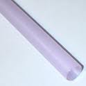 A neodymium-doped YAG laser rod is shown to the left - note its pale pink color. It's an Yttrium Aluminum Garnet crystal in which some percentage of the yttrium atoms have been replaced by neodymium. In the laser, these neodymium atoms are "pumped" into an excited state by focusing the light of two thousand-watt linear tungsten-halogen lamps onto the rod. The end result was a beam of coherent infrared light with a continuous power of only about ten watts. But being coherent, the beam could be accurately focused into an extremely small spot of only about 0.0012 cm (3 mils) in diameter, concentrating quite a bit of heat into a very small spot. Although this was absorbed by the black resistive paste, and was hot enough to melt it, it was reflected by, and did not damage, the ceramic substrate.
 However, just melting the paste was no good - the melted paste would remain more or less in place, and harden as soon as the laser beam moved on. This problem was solved by one more component, an acousto-optic "Q-switch" that was inserted between the laser cavity and the front mirror, as shown in the diagram to the right. In the diagram, the lines labeled "M" represent the rear and front mirrors. The Q-switch and the mirrors were outside the brass laser cavity, which will be discussed below. The Q-switch was a piece of glass, driven by a piezoelectric crystal on one side, which could send a very high frequency (50 MHz) sonic wave through the glass. The changes in the index of refraction that result from that longitudinal pressure wave act as a diffraction grating, and deflect some of the light out of the cavity. This "spoils the cavity", and suppresses the laser action. As a result, virtually all the neodymium atoms are pumped up into the excited state.
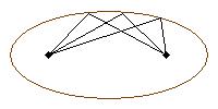 How was all the "pumping" light from the tungsten-halogen lamps focused onto the laser rod? Remember the mathematical properties of an ellipse, which has two points called "foci". If the ellipse is mirrored, light emitted from one focus will be reflected to the other focus, regardless of where it hits the mirrored wall of the ellipse, as shown in the diagram to the left. The diagram represents, schematically, a cross-section of the laser - picture a slice across the laser rod at one of the foci, and a slice across a linear tungsten-halogen lamp at the other focus.
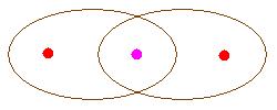 In fact, though, the laser had two lamps, so the cross-section had two ellipses, arranged to have a common focus, at which the laser rod was placed, as shown to the right. This bathed the laser rod evenly in light from both sides, and doubled the amount of pumping energy. Not shown is that the laser rod was surrounded by a glass cylinder carrying chilled water. The laser rod was illuminated with two kilowatts of power, but emitted only about 10 watts as laser light.
 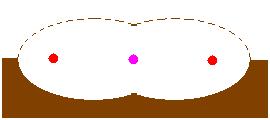 In the image to the left, the brown color shows an approximate cross-section of half of the laser cavity, with an outline of the other half shown by a dotted line. The actual cavity was made of nautical brass, chosen for a low coefficient of thermal expansion. The block of brass was crisscrossed internally with channels for cooling water. The inner reflective surface was plated with gold, a good reflector of light, as well as being non-tarnishing even at high temperatures.
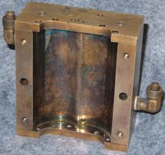 And so, my one remaining souvenir of Micronetic Systems, other than many memories, is one of these half laser block assemblies, shown to the right.