 On May 7, 2019, I participated in a tour of the new MIT.nano building on the MIT campus. The tour was arranged by the MIT's Venture Mentoring Service, where I am a volunteer mentor. The MIT.nano building is Building 12, in the middle of the campus, not far from the Great Dome. It's devoted to nanotechnology research and education. Click here to learn more about MIT.nano. Here's a picture of the building:  During the tour, I was astounded to find a picture on a hallway wall with my name on it, along with the names of some other select individuals! You'll need to read on to find out why I was thus honored. I've observed over the years that people at MIT often do things just for fun, or just because they can. An early art project done in the MIT.nano building is called One.mit. It created a six-inch silicon wafer with an image of MIT's Great Dome etched into it: 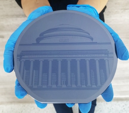 But if you look closely (it takes a microscope), you can see that the image comprises a list of names. In the darker areas of the image, the names are displayed in a bold font, while in the lighter areas, they are displayed in a normal font. Back up a bit, and the image of the dome emerges.
So, whose names are displayed? What did I have to do to become a member of the group so honored? In fact, the wafer displays the names of the more than 270,000 people associated with the Institute from its founding in 1861 up until the Spring of 2018. All I had to do to get on this select list was to graduate from MIT, which I did in 1963. A bit more detail: the silicon "wafer" is the sort of wafer that is ordinarily used in fabricating integrated circuits. Normally, multiple versions of the same circuit are fabricated on a wafer all at once, running the wafer through multiple processing steps (hundreds of steps, actually). The wafer is then scored, and broken up into individual rectangular integrated circuits, called "dice", which are then tested and packaged. The singular of "dice" is "die"; another word for these dice is "chips". Cut open an old credit card, and you can find one inside. But that's a very small chip. A larger chip might contain an entire microprocessor, with trillions of transistors. Or it might contain a gigabyte of dynamic memory. But for this art project, the entire six-inch wafer was used to display a single image. With over 270,000 names, of course, it would seem that there would be no hope of me actually finding my own name on the display. But that's not the case. All I needed to do was to go to the web site http://onemit.mit.edu/, which I did on the spot using my smart phone, while still on the tour. I typed in my name, "Lawrence Krakauer", and two names appeared below it: 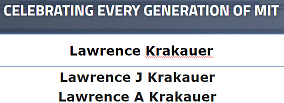 In various other blog entries,Note 1 I've already discussed the fact that there's another "Lawrence Krakauer" with an MIT degree, who happens to live in the same town as I do, Wayland, Massachusetts. That's why two names popped up when I entered "Lawrence Krakauer" on the OneMIT site. But my middle initial is J, so I clicked on that name, and got:  The red box shows where on the image my name is located. Then, scrolling to the right as suggested, I could zoom in: 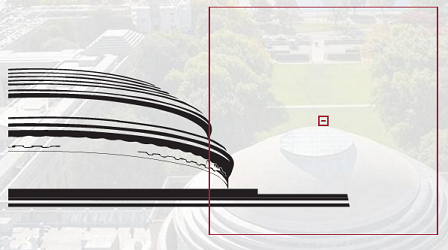 And then zooming again: 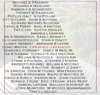 Our tour guide, Tom Gearty (MIT.nano Director of Communications), had noted that even at this level of zoom, it can be hard to find your name on the display. But my name happened to be along the upper-right circular border of the printed area of the image, and that made it easier to locate. He scanned down that border, and found it. Because my name is along the edge of the printed area of the wafer, it's in an area with no dark lines. Thus all the letters of my name, and the names around it, are in a normal (not bold) font. After returning home, I looked up the name of my classmate Mike Bertin, who is Class Secretary of the MIT Class of 1963. It proved to be along the right-hand edge of a portion of the dome, so you can see how bold characters are used to make up the darker parts of the image: 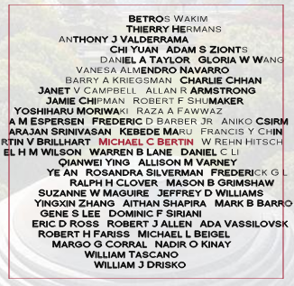 The One.MIT page doesn't explain what determined the order of the names used. It seems rather random to me, and certainly isn't alphabetical. I find it astounding that MIT is able to even generate this list - every student, every faculty member, every staff member, and perhaps every employee, since 1861. If you want to play with this yourself, and you know the name of someone with an MIT affiliation (perhaps yourself), just go to http://one.mit.edu. The wafer I described above is the "OneMIT 2018" wafer, depicting an image of MIT's great dome atop Building 10. To find the desired name on that wafer, click on "Search OneMIT 2018". Apparently, since I wrote this blog entry in 2019, another similar wafer has been created with an image of the MIT seal. To find the desired name on that one, click on "Search OneMIT 2020". In either case, type a name into the box, and see what happens. If you don't know the name of anyone affiliated with MIT, take a look at my blog entry MIT people, where you can find some names you can use. By the way, at the top of that entry, there's a picture of the Great Dome that's depicted on the One.MIT 2018 wafer. It's shown lit up at night. In my experience, MIT people have often pulled off innovative stunts like this just because they're fun to do, and they showcase technology. I described another such effort done years ago in my blog entry Amateur subway riding. I love MIT - you can see why I spent eleven years there.
  Note 1:
My longest story about the other Larry Krakauer in Wayland is the last story in my entry Doctor's office (bis). But he was also mentioned in the entries Google and Krakauer. [return to text]
 |
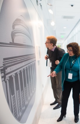 Because the names on the actual wafer are so small, a blown-up image is displayed alongside the actual wafer. You can see a picture of it to the left. I'd guess it's a bit less than 3 meters in diameter. Even thus blown up about 20 times, the names are tiny, but with that magnification, they are big enough to be read with the naked eye.